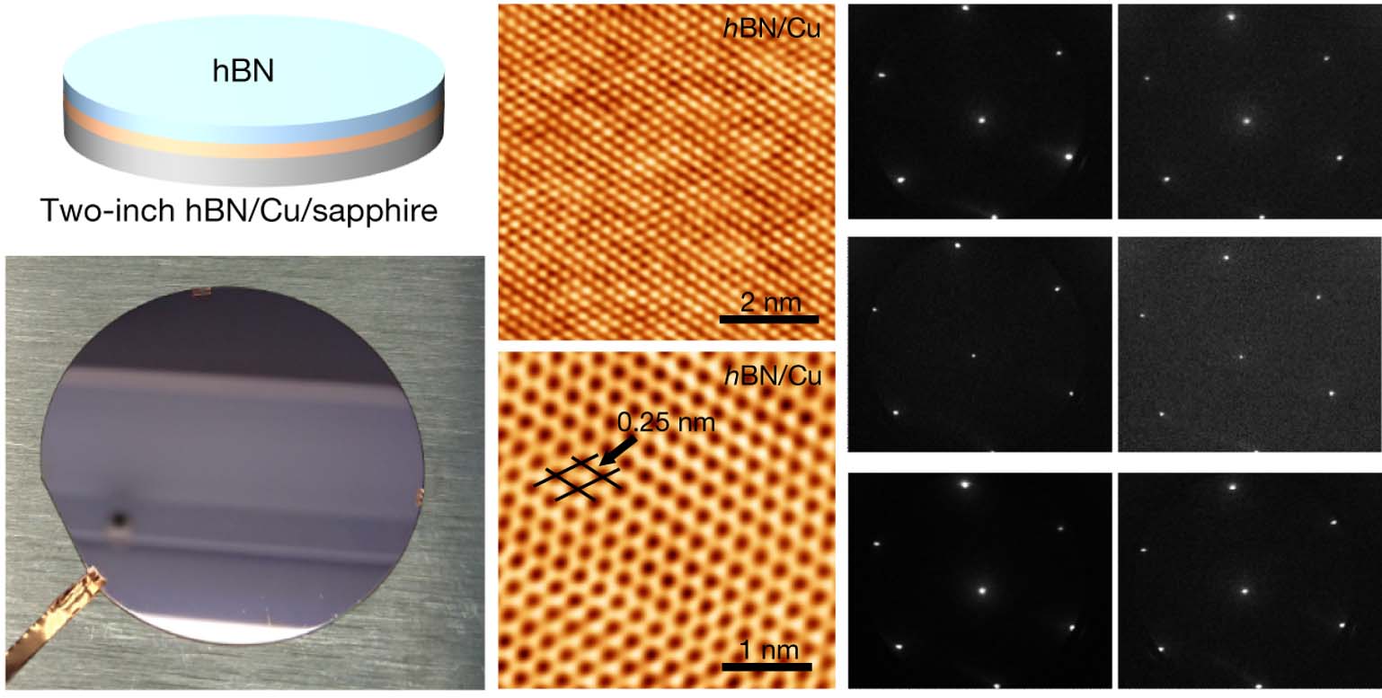
A research team led by Prof. Qiang FU from Dalian Institute of Chemical Physics (DICP) of the Chinese Academy of Sciences in collaboration with Prof. Lain-Jong LI from Taiwan Semiconductor Manufacturing Company (TSMC), Prof. Wen-Hao CHANG from National Chiao Tung University, Prof. Boris I. YAKOBSON from Rice University and Prof. Yanfeng ZHANG from Peking University reported the successful epitaxial growth of single-crystal hexagonal boron nitride (hBN) monolayers on a Cu (111) thin film across a two-inch c-plane sapphire wafer. The results were published in Nature (Nature, 2020, 579, 219; https://www.nature.com/articles/s41586-020-2009-2) on March 4.
Ultrathin hexagonal boron nitride is expected to be one of the best candidate materials for future 2D electronics. However, reliable production of wafer-scale single-crystal hBN films which are compatible with advanced microelectronics fabrication processes still remains a challenge. The joint research teams first deposited 500 nm thick single-crystal Cu(111) thin films without any twinned grains on c-plane sapphire wafers. Single-crystal hBN monolayers were epitaxially grown on the inch-sized substrates. Scientists in DICP used a deep ultraviolet laser photoemission electron microscopy and low-energy electron microscopy (DUV-PEEM/LEEM) system developed by the State Key Lab of Catalysis to characterize the single crystalline quality within the large-area monolayer film. By making use of the unique micro-region surface imaging and surface diffraction capability of the setup, the whole hBN monolayer has been revealed to be unidirectionally aligned with the Cu (111) surfaces by probing around one hundred micrometer-sized spots across the one-inch hBN wafer confirming the single-crystallinity of the hBN monolayer films.
This work was financially supported by the National Natural Science Foundation of China, the Strategic Priority Research Program (B) of the Chinese Academy of Sciences, and National Key Scientific Instrument and Equipment Development Project. (Text and image by Rongtan LI)